Wednesday, July 21, 2010

Electronics


Very High-Tech electronics demand products  that optimize performance. For years, Nanophase has suplllied the innovative products that achieve superior result and allow our customers to develop next generation electronics tecnology.

Optical Glass Polishing

NanoArc® Cerium Oxide has proven to be the best Precision Polishing material for glass surface with respect to surface finish and low detectivity.  In critical applications, such as photomasks and disk drives, surface roughness values of less than 2 angstroms have been achieved. Nanophase products provide the next level of performance for ultra fine polishing applications.

CMP Polishing 

NanoArc® Cerium Oxide provides low defectivity, selectivity and high planarization for direct Shallow Trench Isolation CMP and NanoArc®Aluminium Oxide can be used for metal and dielectric polishing applications in CMP.
Conductive Materials


Nano ITO, ATO | Conductivity
NanoArc®Indium Tin Oxide and NanoArc® Antimony Tin Oxide are transparent materials that reduce resistivity or provide Conductive and can be applied using traditional printing techniques, eliminating the need to use expensive sputtering technologies.

Tuesday, July 20, 2010

Images for Carbon Nanotube

Image 1


Image 2


Image 3


Image 4

Saturday, July 17, 2010

New Iphone 2011


*BIG IPHONE
*SMALL IPHONE
*VERY SMALL IPHONE


*NEWS IPHONE QWERTY KEYBOARD
*KEYPAD GAME IPHONE
*LIKE KEYPAD NINTENDO DSL

Monday, July 12, 2010

Nanotube Electronic


Microscopic wires of the future could be made from carbon nanotubes--rolled-up sheets of graphite only angstroms in diameter. Nanotubes could also be made into electronic devices like diodes and transistors, which are traditionally made from junctions of two or more semiconductors having different electrical properties. In the21 June PRL a team reports their calculations of the basic current and voltage relationships for nanotube junctions, showing that nanotubes should indeed be useable for diodes and other electronic components, once the fabrication techniques improve.
David Tománek of Michigan State University in East Lansing calls nanotubes "dream materials" for building tiny circuits: They're strong, nonreactive, tolerant of extreme temperatures, and pass current essentially without resistance. They're also much smaller than any wires in today's electronics. Surprisingly, nanotubes can have either metallic or semiconducting properties, depending on their geometry: Starting with the all-carbon honeycomb lattice of graphite, you can roll either type of material depending on the direction of the cylinder's axis compared with the lattice.
Electronic amplifiers, switches, and computer logic elements are all made from combinations of semiconductor junctions--interfaces between pairs of materials with differing concentrations of the current carrying electrons and holes. In semiconductors, a simple junction makes a diode, which carries current in only one direction. Researchers have already manipulated the carrier concentrations in nanotubes, so Keivan Esfarjani and his colleagues at Tohoku University in Japan decided to investigate the most basic properties of simple nanotube junctions, to see how they might be suitable for use in circuits.
The team calculated the current transmitted for a range of applied voltages for nanotube junctions with several different geometries and found two useful properties. First, for semiconducting junctions, they found a range of voltages where no current would flow, and the range was not symmetric about zero voltage--exactly the property needed to make a diode. Second, for metallic junctions, they found regions of "negative differential resistance," where increasing the voltage led to lower current--a property useful for other types of electronic components.
Team member Amir Farajian explains that there are two main obstacles to observing these effects in the lab. Although researchers know of ways to "dope" nanotubes to change the electron and hole concentrations, no one has yet made a junction of this type, which requires different doping on two parts of the same tube. The other problem is isolating nanotubes small enough to work. The calculations assumed nanotube diameters of 5.5 Ã…, and they showed that the effects become weaker with larger diameters.
Tománek says the work is another step toward making real nanotube-based electronics, an idea that "people have been discussing for a long time." Only within the last two years have researchers begun to investigate the transport properties of nanotubes, he says, but since then "the progress has been astonishing."

Thursday, July 1, 2010

Process Development Challenges in Difficult Economic Times


Abstract

It is no secret that the semiconductor industry and other high-tech industries like the MEMS and NEMS industry have suffered over the past year. According to figures from the GSA, semiconductor sales were down by 6% in 2008 compared to 2007. Nor is it much of a secret that many industry figures have championed innovation as the key for companies to ride out the storm and indeed to prepare for the upturn when it comes. Most high-tech industries, which are particularly suffering in the current climate, have experienced a downturn in sales. As such, driving down costs is obviously essential in these tough times. However, some long term cost savings have been largely unexplored by high tech companies until now. In particular, the semiconductor, MEMS/NEMS and photovoltaic industries have the potential to decrease time-to-market and the cost of product development by investing wisely in tough times.
This paper investigates the challenges, discusses some important considerations and highlights potential methods for companies to come out of this crisis stronger. The value of specialised software, called Process Development Execution Systems (PDES), will be discussed. A PDES helps to cope with the challenges of growing complexity, shorter time-to-market and development inefficiencies. The paper will demonstrate that the demands to grow future markets with increasingly complex products can only be fulfilled through the intensive use of PDES software like XperiDesk working together with product engineering methodologies. It will be shown that the tools and methods give companies a competitive advantage by developing better solutions and shorterning time-to-market.

Introduction

The economic crisis is currently demanding the lowest possible development costs. These demands are easy to understand but in practice very hard to achieve. Tight time limitations and the use of the wrong tools, or no tools whatsoever, make the situation more difficult to resolve. Added to this, the complexity of process development increases every day.
More technology options, material choices and suppliers complicate matters even further. Now, more than ever before, new data management strategies need to be implemented to help deal with the challenges. Employing intelligent software support is one potential solution that can offer many benefits. However, the vast amount of development data is difficult to manage. To avoid getting lost in an ocean of information, an intelligent solution covering the full development loop, indicated in Figure 1, is required.

On the other hand, cash is king nowadays. So is the timing really right to invest into new strategies while old strategies are more or less still applicable? Some leading industry figureheads have championed innovation as the key for their organisation to ride out the storm and indeed to prepare for the upturn when it comes.
It is very difficult to disagree with this viewpoint, innovation is crucial to any company, recession or not. However, when thinking of innovation, it is often only the straightforward and tangible implications that are considered. People often associate innovation with new products or new strategies. What is often underestimated is that the main challenge for engineers now is the increasingly complexity of new technologies combined with the need to develop and deploy these technologies within a much tighter time scale at an increasingly competitive price. To meet these challenges innovation needs to go a lot deeper into a company.

Main Challenges

The main challenge for engineers is dealing with new technologies which are increasingly complex, whilst having to commit to developing products within a much tighter time scale at an increasingly competitive price. Over the past twenty years, there has been a focus on shortening cycle times in manufacturing. The widespread use of various statistical tools such as 'Statistical Experiment Design' has enabled this development to continue.
However, there are physical limits to development time and the semiconductor industry in particular is fast approaching them. If we want to keep up this rapid development of ever more intelligent and function rich ('More-than-Moore's Law'), yet low cost chips, new technologies and materials need to be employed. The process development stage of thin-film developments has obvious scope for improvements as introduced in more detail in Ref 
For example, by utilising existing knowledge to its fullest, the number of experiments that need to be performed can be limited. Those that remain can be simulated first rather than being performed physically immediately. Finally, all the results gained from the experiments can be automatically collected using a structured process to develop a knowledge base for future use. Planning with such techniques can reduce the time spent iterating development steps.
Collaboration between different people and groups inside or outside a company is imperative for high tech developments. This can include collaboration between different groups around the globe. Market trends and development costs even drive the need for collaborative development activities between different legal entities.
Collaboration can improve the time-to-market. However, a proper central development platform, including communication and electronic knowledge transfer functionalities, is needed to do so efficiently. Historical data must be recorded and shared otherwise the mistakes of the past will be repeated.
Experts in semiconductor process development estimate that 10-15% of failed and retaken experiments could be avoided if previous results were accessible. It is vital to document everything - every idea, project, experiment, meeting, and conclusion. If this is done successfully and effortlessly, engineers can draw optimum results from new results. New and existing data can be correlated and thus new information can be exposed. For example, PDES can build up a network of imperative information that will not only benefit current developments, but it will be useful in future process developments too.
Another challenge often encountered is the transfer of manufacturing processes from research into production. Once the experiment and development process has been streamlined, a Manufacturing Execution System (MES) should be implemented, to assist with the extensive production process. However, it is only as good as the input it receives. If the program is cluttered with unnecessary experiments, the cycle time will inevitably increase. A key benefit of implementing a system such as the PDES XperiDesk is that it enables manufacturers to run less wafers in the fab. As a result, it frees up valuable resources, saves money and significantly reduces the probability of equipment downtime.
Documenting and reporting the development progress can be tedious at best. Cluttered results storage burdens development engineers with major manual effort, requiring them to manually collect data from diverse machinery. Additionally the assembly of the collected result data into reports and the evaluation can take a major part of engineering time. Industry experts report that up to 80% of engineering time is spent on data collection and arrangement rather than on data evaluation. Even if the average is much lower, it is still a major part of the working time spent on tedious and error prone tasks.
Automising these can inject creativity back into the development process. Reporting on the development status is often more of a manual assembly of the reports rather than an automated process. The input data is often not up to date so that the work in progress (WIP) status is not necessarily precise. The impacts of these effects are even aggravated by quality assurance and compliance demands such as ISO 900X, CMMI, SOX etc. Because those apply more and more in development as well as in production, there is a strong demand to fulfil the imposed documentation requirements.
To summarise, making cost reductions in process development can be achieved by following four basic rules:
  1. fully utilise existing knowledge,
  2. learn in a different way (e.g. by simulations),
  3. gain more information from your experiments, and
  4. transfer all required knowledge to production.

Introducing Software Support

These rules are key while facing the current economic climate. But the question arises whether the timing is right to introduce new software to support the associated tasks now. When developing new products or technologies what many people fail to consider is the Total Cost of Ownership (TCO). This refers to the full burden of costs involved in development and innovation. TCO goes far beyond the usual costs, overheads and staff costs. It also incorporates all of the costs involved with acquiring new or better machinery, the HR costs of taking on new staff, the costs of adopting new methodologies and even activities such as staff training that are often overlooked. This is the depth of innovation this paper refers to. It is not enough to develop a new product. Rather, in order to engender long term innovation and commercial success, companies need to be looking at a much bigger picture.
What is more, there is a huge advantage to dealing with these issues during an economic downturn: costs are lower during a recession; generally it is a time when companies will be operating with reduced staff levels; and lastly during a recession there will be, generally speaking, more bandwidth and resources available within a company. The findings of a McKinsey study of the 1990-91 recession show how companies can take advantage of these circumstances.
The study found that companies that remained market leaders or became serious challengers during the downturn had done so by increasing their acquisition, R.&D., and ad budgets, while companies at the bottom of the pile had reduced them. Certainly there are already companies that take advantage of these circumstances; IBM has a stated policy to invest during downturns - in people, in training and in technology. But it is not necessarily a widespread philosophy. Most companies understandably view downturns as a time for cost cutting and a rationalisation of activities. However, to introduce these disruptive technologies and methodologies internally, there is no better time than during an economic downturn.
Not only are the costs of new machines, software or technology lower during a downturn, but also a whole raft of other cost savings can be made. For instance, during times of reduced staff, introduction costs and hurdles for new systems or procedures are much lower. Moreover, instituting more staff training during a downturn, when staff levels are lower, is a significant cost saver. And more generally in economic downtimes more resources are available for evaluating current practices and learning about new ones. During an upturn there is very little bandwidth, in terms staff availability and time pressures, for introducing these new technologies, procedures or training courses.
Companies need to prepare for the next upturn, and in recent months there have been more positive economic signs. Future Horizons' latest Global Semiconductor Report shows that April 2009 had the strongest month-on-month growth for April since 1996. Ultimately companies have to find ways of doing more with less (during a market or production rise companies will generally have fewer engineers than at the peak of the market).
Of course, new products and new ideas are what will ultimately deliver the commercial success technology companies desire, but where will these products and ideas come from? These things cannot be left up to chance and investing in an organisation, its infrastructure and its staff has the potential to give a significant head start.

Conclusions

This paper gave a brief overview of current process development practices and challenges with a focus on possible improvements using better software support. Additionally it highlighted aspects of introducing such software support and the impacts and timing of the introduction. According to results of McKinsey studies investigating the impacts and strategies of investing during challenging economic times, the timing is right to change the development strategies in tougher times rather than during rising or peak times. Better software support can be achieved by introducing a Process Development Execution System such as XperiDesk (a commercially available implementation of a PDES) which supports the whole development flow - from the first device idea to the transfer of the resulting recipe into production or to a collaborating partner.

References

1. K. Hahn, T. Schmidt, M. Mielke, T. Brück, D. Ortloff: Micro and Nano Product Engineering using Data Management for Silicon-based Fabrication Process Development. In: Proceedings of the 9th IEEE International Conference on the Nanotechnology, Geneva, 2009.
2. D. Ortloff, J. Popp, A. Wagener: Recurring deficiencies in process development support. In: Proceedings of the 13th International Conference on the Commercialization of Micro and Nano Systems, Puerto Vallarta, 2008.


Progress and Perspectives in the Carbon Nanotube World

Over the last decade, nanotechnology has received lots of attention from within society as a potential source for novel solutions to many of the world's existing and emerging problems. Simply put, nanotechnology could provide the ability to better understand and design complex solutions on an atomic and molecular scale. The most attractive nanotechnology-related nanomaterial is considered to be one-dimensional carbon nanotubes (CNT).
Geometrically, CNT can be visualized by rolling sheets of graphene into a long hollow tubule. The unique configuration of this material imparts excellent physico-chemical properties1. For instance, the Young's modulus of CNT is stiffer than any other material, while their tensile strength is 100 times that of steel. Maximal electrical current density is 100 times greater than for copper wire and carrier mobility is ca. 105 cm2/Vs. CNTs show great promise in numerous applications in the near future2 and the excellent properties of CNT have already resulted in their use in commercial available products.
At present, the total amount of CNTs produced commercially from around the world reached ca. 1,000 ton/year. In this feature article, the basic structure of CNTs is briefly described, as well as the latest advances in the large-scale production, existing commercial uses of nanotubes are reviewed with special emphasis on the toxicological issue of CNTs.

What is a Carbon Nanotube?

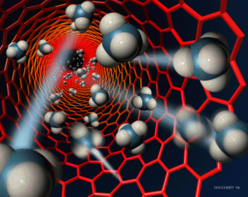
CNT can be visualized as rolling sheets of graphene (sp2 carbon honeycomb lattice) into a cylinder of nanometer size diameter (Fig. 1 (a)). The structure of CNT has been explored in the early years with high-resolution transmission electron microscopy (Fig. 1 (b))3, and the results obtained reveal that nanotubes are seamless nanoscale tubules derived from the honeycomb lattice representing a single atomic layer of crystalline graphite, otherwise referred to as a graphene sheet. The curvature of the nanotubes incorporates a small amount of sp3 bonding so that the force constant in the circumferential direction is slightly weaker than along the nanotube axis.


Figure 1. (a) CNT could be visualized by rolling sheets of graphene (sp2 carbon honeycomb lattice) into a cylinder of nanometer size diameter. (b) The structure of CNT has been explored early on by high-resolution transmission electron microscopy .
Since single-walled carbon nanotube (SWNT) is only one atom thick and has a small number of atoms around its circumference, only a few wave vectors are needed to describe the periodicity of the nanotubes. These constraints lead to quantum confinement of the wave functions in the radial and circumferential directions, with plane wave motion occurring only along the nanotube axis, corresponding to a large number or closely spaced allowed wave vectors.
Carbon nanotubes can be either metallic or semiconducting, and likewise the individual constituents of multi-wall nanotubes or single-wall nanotube bundles can be metallic or semiconducting4. These remarkable electronic properties follow from the electronic structure of 2D graphite under the constraints of quantum confinement in the circumferential direction.
In the case of multi-walled carbon nanotubes (MWNTs), which typically have a diameter less than around 100 nm, no graphitic three-dimensional stacking is established5, even though an individual shell of the multi layers consists of perfect graphene sheets. Also, each tube has different and independent chirality, which might contribute to a larger inter-shell spacing than is found in graphite. These characteristic structures of single- and multi-walled CNTs indicate that they are unique one-dimensional materials with fascinating electronic, chemical, mechanical, and thermal properties.

Industrial Scale Production of Carbon Nanotubes

Up until now, various synthetic methods for producing CNTs have been reported (e.g., arc discharge, laser vaporization and catalytic chemical vapor deposition (CVD)). The dominant recent trend is to synthesize CNTs using CVD approach since this technique is extremely useful for the large-scale production of both SWNTs and MWNTs3. By simultaneously feeding hydrocarbons and nanoscale catalytic particles in the gas phase into the reaction chamber, CNTs have been synthesized on a large-scale6.
Growing SWNTs and MWNTs in a reactor has been proposed and this involves the catalytic deposition of hydrocarbons over the surface of nano-sized metal particles and a continuous output by the particle of well-organized tubule of hexagonal sp2-carbon3,6. The strong evidence of this assumption is the presence of catalytic particles at the ends (top or root) of the tubes (Fig. 2 (a-c)). In the case of large-scale production of SWNTs, the development of the high-pressure carbon monoxide process gave impetus to the scientific study and applications of SWNTs7.
Figure 2. shows the presence of catalytic particles at the ends of the tubes.
Regarding the bulk production of MWNTs for industrial applications, it is important to mention that at the end of 1980, Showa-Denko Co. Ltd and Hyperion Catalysis International, Inc. (Cambridge, MA) commenced production of several tons of catalytically grown CNTs annually. At present, the total amount of the commercially available MWNTs around the world has reached 1,000 ton/year. It is expected that the global carbon-nanotube revenue in 2015 will reach US$500 million8. The most interesting point is that all companies selected a catalytic CVD method for the large-scale production of MWNTs.

Application of Carbon Nanotubes

Due to their small dimensions and excellent physicochemical properties, CNTs have been proposed for a wide range of applications. Some of the potential applications of CNT include multi-functional composites, electrochemical electrodes and/or additives, field emitters as well as nano-sized semiconductor devices2. CNTs are also used as fillers in both anode and cathode materials of lithium-ion secondary batteries9,10.
MWNTs can be used as scanning probe microscope tips to obtain high-resolution images and in the near future, thin MWNTs will be used as field emission electron sources for flat-panel displays. Chemically functionalized MWNTs also give a high sensing ability for chemical and biological groups interacting with different surfaces.
In addition, CNTs are an ideal candidate for fillers in polymer composites. The smallest working composite gear has been prepared by mixing nanotubes into molten nylon and then injecting into the tiny mold. This piece exhibits a high mechanical strength, high abrasion resistance and also good electrical and thermal conductivity. Further progress has to be carried out in order to fully utilize these nanotube/polymer composites, for example the optimization of surface properties, the homogeneous dispersion without physical damage, the development of an effective alignment method (also evaluation method) and processing.
A super rubber sealant capable of withstanding high temperature and pressure was successfully fabricated by Professor Morinobu Endo and his colleagues at the Institute of Carbon Science & Technology. This was done by incorporating surface-modified nanotubes into rubber11. Based on our estimates and after surveying the depth and temperature of oil resources, the development of a super rubber technology capable of withstanding 260°C under 239 MPa of pressure will contribute to a revolutionary enhancement in oil recovery efficiency from the current 35 % to more than 70 % by excavating previously inaccessible deposits.
Another potential application of CNT is in the fabrication of super-capacitors and electrochemical actuators used in artificial muscles. Nanotube actuators can operate at low voltages and temperatures as high as 350°C. Currently, super-capacitors are incorporated into hybrid vehicles as they could provide rapid acceleration and store breaking energy electrically.
The possibility of using CNTs as nanowires is envisaged due to their observed ballistic transport. For the fabrication of nanotube field effect transistors, SWNTs were connected to metal nano-electrodes. The performance is excellent in terms of switching speed owing to their low capacitance. An inherent problem associated with CNT lies in the difficulty in manipulating them. From a commercial viewpoint, further technical progress is required, such as selective growth of nanotubes using self-assembly techniques.

Carbon Nanotube Biocompatibility

Much attention was paid on the toxicity of CNTs due to their nanoscale dimension and their morphological features similar to that of asbestos12,13. Therefore, toxicological evidence of CNT is strongly needed to prevent risks and occupational disorders in workers and to promote their safe use in consumer products. Our preliminary studies on the biological response of CNTs indicates their potential toxic nature is significantly low14,15. However, a more thorough and long-term study has to be conducted to determine the toxic nature of various types of CNTs such as direct aspiration of tubes in human lungs.

OUTLOCK
These tiny, black and tubular-type nanomaterials will change the way we live, work and communicate. A large number of CNT-derived products are already in use and their viability strongly depends on the success of their commercialization.
Before considering the use of CNTs in commercial products as a success, at least four obstacles have to be resolved:
   1. How to obtain high purity CNTs as metallic impurities often remain after the fabrication process which can give rise to toxic properties.
   2. How to manipulate these tiny materials.
   3. How to control the chirality of CNT.
   4. The most important but critical "safety" issue has to be clarified based on long-term and systematic biological studies.
Extensive and intensive efforts in both academy and industry are looking for a solution to these obstacles and once a solution has been reached, CNTs will play a key important role as an innovative material of 21st century in a number of industrial processes.
We have reached beyond the first mountain of science, the second mountain of technology and the third mountain of economy by producing CNTs successfully on a large-scale at reasonable cost (Fig. 3). Now we are striving to climb the mountain of society. By sharing information on risks and benefits of CNTs with all stakeholders, we will finally reach the top of a nanotube mountain and prove CNT is an innovative material for the 21st century.
Figure 3. Carbon nanotube as a leading-edge of nanotechnology must go beyond the four mountains as an innovative and fundamental technology of 21st century. Worldwide collaboration on science is the key issue for the success.

Acknowledgement

This work was in part supported by the CLUSTER (second stage) and MEXT grants (No 19002007), Japan.

References

1. M.S. Dresselhaus, G. Dresselhaus and P.C. Eklund, Science of Fullerenes and Carbon Nanotubes, Academic Press, San Diego (1996).
2. M. Endo, M. S. Strano, P. M. Ajayan, In Carbon Nanotubes: Advanced Topics in the Synthesis, Structure, Properties and Applications (Eds, A. Jorio, M. S. Dresselhaus, G. Dresselhaus), Springer, 2008, pp 13-61.
3. A. Oberlin, M. Endo and T. Koyama, J. Crystal Growth 32, 335-349 (1976).
4. R. Saito, M.S. Dresselhaus and G. Dresselhaus, Physical Properties of Carbon Nanotubes, Imperial College Press, London (1998).
5. X. Sun, C.H. Kiang, M. Endo, K. Takeuchi, T. Furuta and M.S. Dresselhaus, Phys. Rev. B 54, 1 (1996).
6. M. Endo, Chem. Tech. 568-576 (1988).
7. P. Nikolaev, M. J. Bronikowski, R. K. Bradley, F. Rohmund, D. T. Colbert, K. A. Smith, R. E. Smalley, Chem. Phys. Lett. 313, 91 (1999).
8. Business Watch, Nature 461, 703 (2009).
9. M. Endo, Y.A. Kim, T. Hayashi, K. Nishimura, T. Matushita, K. Miyashita and M. S. Dresselhaus, Carbon 39, 1287-1297 (2001).
10. C. Sotowa, G. Origi, M. Takeuchi, Y. Nishimura, K. Takeuchi, I. Y. Jang, Y. J. Kim, T. Hayashi, Y.A. Kim, M. Endo, M. S. Dresselhaus, ChemSusChem 1, 911-915 (2008).
11. M. Endo, T. Noguchi, M. Ito, K. Takeuchi, T. Hayashi, Y.A. Kim, T. Wanibuchi, H. Jinnai, M. Terrones, M.S. Dresselhaus, Adv. Funct. Mater. 18, 3403-3409 (2008).
12. A. Takagi, A. Hirose, T. Nishimura, N. Fukumori, A. Ogata, N. Ohashi, S. Kitajima, J. Kanno, J. Toxicol. Sci. 33, 105-116 (2008).
13. C. A. Poland, R. Duffin, I. Kinloch, A. Maynard, W. A. H. Wallace, A. Seaton, Nat. Nanotech. 3, 216-221 (2008).
14. S. Koyama, M. Endo, Y.A. Kim, T. Hayashi, T. Yanagisawa, K. Osaka, H. Koyama, N. Kuroiwa, Carbon 44, 1079-1092 (2006).
15. S. Koyama, Y.A. Kim, T. Hayashi, K. Takeuchi, C. Fujii, N. Kuroiwa, H. Koyama, T. Tukahara, M. Endo, Carbon 47, 1365-1372 (2009).
Copyright AZoNano.com, Professor Morinobu Endo (Shinshu University)
Date Added: Jun 23, 2010 

Thin-Film Material Increases Power Production in Fuel Cells

This diagram shows the experimental setup used by Prof. Yang Shao-Horn and her team. The circles in the background represent tiny thin-film electrodes made of a material called strontium-substituted lanthanum cobalt perovskite, or LSC (whose crystal structure is diagrammed at top left). The diagram shows the lab setup used to measure the catalytic activity of the LSC. The circular cutout shows how oxygen molecules (O2) are exchanged on the LSC surface. 
Illustration by postdoctoral researcher Eva Mutoro
This diagram shows the experimental setup used by Prof. Yang Shao-Horn and her team. The circles in the background represent tiny thin-film electrodes made of a material called strontium-substituted lanthanum cobalt perovskite, or LSC (whose crystal structure is diagrammed at top left). The diagram shows the lab setup used to measure the catalytic activity of the LSC. The circular cutout shows how oxygen molecules (O2) are exchanged on the LSC surface. Illustration by postdoctoral researcher Eva Mutoro

In many cases, thin layers of a material- which may be just a few molecules in thickness -exhibit properties different from solid blocks of the same material. But even though this is a known phenomenon, the nature of the difference the MIT team found in the behavior of thin films of a mineral called perovskite - in this case, deposited as a thin layer on the surface of a crystal of zirconia - “was very much unexpected,” says Yang Shao-Horn, associate professor of mechanical engineering and materials science and engineering at MIT, who led the research. The work was done in collaboration with Hans Christen and Michael Biegalski at Oak Ridge National Laboratory.
In fuel cells, a fuel such as hydrogen or methanol reacts in the presence of a catalyst, releasing its energy chemically rather than being burned. As a result, they can produce electricity from fuel without releasing greenhouse gases or other pollutants, and so are considered a promising alternative approach for generating electricity. And unlike batteries, which need to be recharged in a time-consuming process, a fuel cell can be refueled quickly.
The main barrier to achieving greater efficiency in fuel cells, which are considered a promising way of supplying electricity for future transportation or stationary power systems, is the slow rate of oxygen production from the cathode, one of the two electrical terminals in the device. In present fuel cells, the rate of oxygen production is the limiting factor in the power output of the device. Many teams are pursuing ways of improving the efficiency and reducing the costs of the two major kinds of fuel cells: solid-oxide fuel cells (SOFCs) and proton-exchange membrane fuel cells (PEMFCs). This work addresses potential improvements in the cathode in SOFCs, which could find application in large-scale systems such as electric power plants. The new research suggests that this activity can be increased by up to a hundredfold by using thin films of certain perovskite compounds.
Previous research had found the opposite, that thin films of some perovskite materials were a hundred times less reactive than the bulk material, Shao-Horn says. The new results are published online in the German journal Angewandte Chemie; the lead authors are former student Gerardo la O’ and postdoctoral researcher Sung-Jin Ahn. The work was supported by the NSF, the U.S. Department of Energy, Oak Ridge National Laboratory and the King Abdullah University of Science and Technology.
By creating the kind of high-purity thin films of material used in this study - in this case, as thin as 20 nanometers, or billionths of a meter - it is possible to study the details of how the surface of the material reacts in much greater detail than has been possible in research with bulk materials. This research shows that unique thin-film characteristics can enhance catalytic activity.
“To our knowledge, this is the first time these thin films have been shown to exhibit” the increased activity, Shao-Horn says. The team is continuing research to verify their hypothesis about the reasons for the increased activity, and to explore a family of materials that may exhibit similar properties. “We are working on determining why” the activity level is so high, Shao-Horn says, suggesting that the increased reactivity of the material may result from a stretching of the surface. This may change the content of oxygen vacancies or the electronic structure of the material, possibilities that are being examined in Shao-Horn’s group.
While many fuel cells use electrodes made from precious metals such as platinum, the electrodes in this experiment are made from relatively abundant materials such as cobalt, lanthanum and strontium, Shao-Horn says, so they should be relatively inexpensive to produce. In addition, this material works at much lower temperatures than existing SOFC electrodes, which could be an advantage because “at lower temperatures, material degradation can be much reduced,” she says. Whereas current cells work at temperatures of 800 degrees Celsius or higher, the new approach might lead to materials that could work at 500 degrees Celsius, as was the case in these tests.
This work is just the first step, however. Shao-Horn stresses that this is the beginning of a new fundamental research area, and could lead to exploration of a whole family of possible compounds in search of one with an optimal combination of high catalytic activity and high stability. This highly reactive material could find a home in places other than fuel cells: for instance, in high-temperature sensors and in membranes used to separate oxygen from nitrogen and other gases, she says.

Buy your own Tron Lightcycle: US$35,000


The lightcycle scene was probably the most memorable part of an absolutely jaw-dropping movie when Tron was released back in 1982. One of the first films ever to use the kinds of computer-generated special effects that later become commonplace, it was a glimpse into a whole new world that left an indelible impression on most that saw it. Now, as Disney prepares to release Tron Legacy, a sequel some 28 years after the original, the lightcycles are back and looking meaner than ever. Built by the same guys that did the memorable Batpod replica, the new lightcycles feature massive dual hubless wheels, carbon fiber/fiberglass bodies and all the lashings of neon that you'd expect. And there's going to be five running models built - all of which are now up for sale on eBay. Check it out!
The lightcycles are to be built by Parker Brothers Choppers, each will be individually numbered from 001 to 005, and each will come with a different color neon highlight. Only five will ever be built.
Buyers can specify what size combustion engine they want, or use a high-powered electric motor to really get in the digital swing of things. Special tires are being made up to fit the enormous 22" x 12" hubless rims - and the manufacturer, Hoosier, will make additional tires available if you wear the originals out - because these lightcycles are being built for street use, not just to be shown.
They're selling for US$35,000 apiece, which is a bit of a steal for something so technically challenging to build - not to mention something that will cause extreme whiplash for the general public, and a stack of dry-cleaning bills for any geek that sees it.

See the eBay auction for more details.

New Toyota Wish 2010


Toyota have launched the new Wish in the Japan market not too long ago, with a new front look.


The new Wish is fitted with the new generation engine with “Valvematic” technology, i guess they renamed VVTL-i to this name, since the technology is variable valve and lift.


The interior looks great, with the triangular window at the side so that you have more view of the road.
This baby also comes with Super CVT-i transmission which gives better fuel economy. Also mentioned is that the 1.8L gives 16Km/L while the 2.0L gives 15.2Km/L. I would say these are pretty impressive figures for the MPV class.
Also available is an Eco Drive mode, i guess in this mode the ECU optimizes the alignment of the driving force with the accelerator operation to offer better fuel economy.
The 1.8L makes about 142 HP with 176 Nm of torque while the 2.0L makes out 156HP with 196Nm of torque.
Have not much idea when will this be available in Malaysia, so which would you choose, the new Wish or the Honda Stream RSZ ? :p
 Wish-03

Search

Custom Search

 
Design by Wordpress Theme | Bloggerized by Free Blogger Templates | coupon codes